In this article I will show my Lanzar amplifier.The amplifier was assembled half a year ago to order, but in the end the customer changed his mind and I abandoned work on it.
I remembered about him only now, when the competition began. The amplifier is almost complete, all that is missing is a couple of field switches in the converter and we need to achieve adequate protection, but everything is ready. Unfortunately, I will not conduct tests of the amplifier in the video, the two main reasons are the lack of a powerful 12 volt power source and the second - the 100 watt test speaker gave up life during the previous tests, the diffuser simply jumped out along with the coil, now I am without a speaker :) for Then I measured the power, at 5 - almost 6 ohms it was 300-310 watts.
One thing that surprises me about this amplifier is that with an output power of almost 300 watts, the output transistors do not burn out, although they were bought on eBay for 100 rubles/pair.
Below is the amplifier circuit
The circuit was taken from the Internet, as was the printed circuit board.
Now let's look at the converter circuit
I drew the circuit myself, here we see a voltage converter on IR2153, the frequency of the converter is 70 kHz, as power transistors IRF3205 was used, 2 pieces per shoulder.
And – the converter’s power can be supplied (through a fuse, of course) directly to the battery, because the converter will turn on only when 12 volts are supplied from the radio to the REM contact, namely to the power leg of the microcircuit. Here's a clever launch scheme. By the way, the cooler is powered not directly from the battery, but from a separate output of the converter specifically so that it turns on only when the amplifier itself is turned on, and does not spin endlessly, which would greatly reduce its lifespan.
The transformer is wound on two folded rings with a permeability of 2000
The primary winding contains 5 turns per arm with 0.8 mm wire in 10 cores. The main secondary winding has 26+26 turns with the same wire of 4 cores. The low-pass filter power winding contains 8+8 turns of the same wire. The winding for powering the cooler is 8 turns.
At the output we have a bipolar voltage of +- 60 volts to power the amplifier itself and the protection unit, a bipolar stabilized +-15 volt to power the low-pass filter, and a unipolar stabilized 12 volt to power the cooler. All voltages are rectified by diode bridges. The main output is 4 FCF10A40 10 Ampere 400 Volt diodes, they are placed on the radiator. The remaining bridges are built from ultra-fast 1 Amp UF4007 diodes.
There is no low-pass filter or protection circuit, but there are printed circuit boards with all component ratings.
This is what I ended up with
Good evening, gentlemen radio amateurs! It all started with the fact that in his home UMZCH had long wanted to abandon cheap TDA-sheks and move to a higher level - a decent transistor audio amplifier. I read many pages of a wide variety of forums, looked through various photo galleries, reviewed reviews... and decided to try to assemble a new one for myself; the choice fell on a very well-known Lanzar amplifier with good characteristics. Then a month was spent studying all possible types of circuits for this amplifier and choosing the optimal one and the one that was suitable in terms of characteristics.Schematic diagram of ULF Lanzar
It seemed to me relatively easy to repeat and customize, although it is the one that gets the most attention on all the forums! Well, I went to the radio market, bought parts, the price cost me 110 UAH - a lot for a student, I’ll tell you, but the end result was worth it, more on that later... I set about making a printed circuit board, with etching took an hour and a half. I poisoned with ferric chloride, I’m not used to it yet since I mainly use it copper sulfate. After preparing the board of the future, Lanzara took up soldering, first of all, jumpers were soldered in, then resistors, capacitors, transistors...

Having soldered the board, we move on to the main thing - setting the no-load current of the UMZCH. Here everything was simple for me - I set the trimmer to the average value, soldered it, checked the board for snot and turned it on. Even without fuses (not like light bulbs). Lanzar started up immediately, drove it for 15 minutes until the VC warmed up, but the trimmer did not pull, measured the voltage drop on the five-watt resistors - it did not change, no noise or other noticeable distortions were detected with an oscilloscope, which showed the high repeatability of this circuit!

Now about the impressions of the sound: earlier when listening tda7294
for at least an hour and the subsequent exception it felt as if a tightly stretched helmet had been removed from my head, then I realized that this was due to a lack of midrange frequencies tda7294
.

Now it’s time to load the lanzar with a pair of low-power speakers, since my power supply is +-22V test, then small 25-watt speakers were just right for it.
Photo of the finished UMZCH

As you can see from the pictures, the power supply capacitors are not very fat, only 470 uF, but in terms of voltage they have a large margin, since it is planned in the future to power Lanzar from +- 65V! These speakers were connected to the amplifier during the setup process.
ULF Lanzar is an amplifier built according to a classical symmetrical circuit, operating in class AB. Many car amplifiers are assembled according to a similar scheme. Simple scheme, the “intelligence” of assembling and tuning this amplifier on numerous forums is a guarantee of success for novice amplifier builders. Enough for hands to grow out of right places, all that remains is to solder everything correctly and set the quiescent current, that’s the whole setup. Therefore, after assembling amplifiers on microcircuits (TDA7294), the next step may well be Lanzar. The sound is quite decent, unpretentious and durable, can be used to work with subwoofers. Bipolar and field-effect transistors can be used as output transistors.
ULF Lanzar circuit

Ever since Interlavka, it became a custom to make Lanzars using this kind of wiring. Uh-uh, in light of the latest trends in PCB wiring, it’s just terrible...

The circuits of the power and ground buses are very long, and the power conductors are thin; they must be routed exactly the opposite way. Although, once upon a time, the first ULF I assembled and worked was Lanzar with all these shortcomings). And then I made some progress in mastering PCB layout in P-CAD, taking into account the recommendations on the forums. The result is Lanzar on field patches, double-sided PP, the top layer is mostly green in the form of a solid polygon. It turned out compact and according to Feng Shui)

Board layout on bipolars with one output pair:

First, we check the correctness of the wiring with LUT, otherwise you will miss the jamb and it will multiply when ordering the PP at the factory... This is how the Lanzar ULF on one pair of bipolars looks assembled. The PP is double-sided, so I had to fiddle with the iron, aligning the printouts to the control points with pins. In general, it worked out fine and the channels launched immediately.

Since there were no errors in the wiring, you can order the PCB from the production, because The series was not planned yet, so to save money without a mask and markings:

The question is regularly asked: “How to wind output coil". Simple: take a drill (mandrel) with a diameter of 5.7-5.8 mm, an enamel wire of 1-1.1 mm, wind 8 turns there and 7 turns back. We clean it, shape it after planting, everything is ready.
Lanzar also split it into two pairs of bipolars, soldered them and launched them half-turned:

The photo was preserved only without the ends, because I didn’t have time to solder it, the amplifier “found” a new owner)

Figure 1 Circuit of the LANZAR power amplifier entirely based on bipolar transistors.
INCREASE

Figure 2 Circuit of the LANZAR power amplifier using field-effect transistors in the penultimate stage.
INCREASE
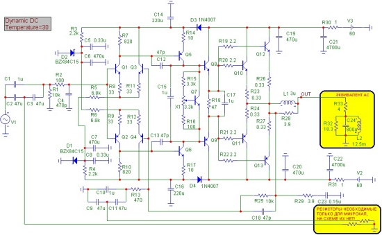
Figure 3 Circuit of the LANZAR power amplifier from the MS-8 simulator. INCREASE
|
LIST OF ELEMENTS INSTALLED IN THE LANZAR AMPLIFIER |
|
|
FOR BIPOLAR OPTION |
FOR THE OPTION WITH FIELDS |
| C3,C2 = 2 x 22µ0 C4 = 1 x 470p C6,C7 = 2 x 470µ0 x 25V C5,C8 = 2 x 0µ33 C11,C9 = 2 x 47µ0 C12,C13,C18 = 3 x 47p C15,C17,C1,C10 = 4 x 1µ0 C21 = 1 x 0µ15 C19,C20 = 2 x 470µ0 x 100V C14,C16 = 2 x 220µ0 x 100V R1 = 1 x 27k VD1,VD2 = 2 x 15V VT2,VT4 = 2 x 2N5401 |
C3,C2 = 2 x 22µ0 C4 = 1 x 470p C6,C7 = 2 x 470µ0 x 25V C5,C8 = 2 x 0µ33 C11,C10 = 2 x 47µ0 C12,C13,C18 = 3 x 47p C15,C17,C1,C9 = 4 x 1µ0 C21 = 1 x 0µ15 C19,C20 = 2 x 470µ0 x 100V C14,C16 = 2 x 220µ0 x 100V R1 = 1 x 27k VD1,VD2 = 2 x 15V VT8 = 1 x IRF640 |
For example, let's take the supply voltage equal to ±60 V. If the installation is done correctly and there are no faulty parts, then we get the voltage map shown in Figure 7. The currents flowing through the elements of the power amplifier are shown in Figure 8. The power dissipation of each element is shown in Figure 9 (about 990 mW is dissipated on transistors VT5, VT6, therefore the TO-126 case requires a heat sink).

Figure 7. LANZAR power amplifier voltage map ENLARGE

Figure 8. Power amplifier current map ENLARGE

Figure 9. Amplifier power dissipation map ENLARGE
A few words about details and installation:
First of all, you should pay attention to the correct installation of parts, since the circuit is symmetrical, there are quite frequent mistakes. Figure 10 shows the arrangement of parts. Adjustment of the quiescent current (current flowing through the terminal transistors when the input is closed to the common wire and the compensating current-voltage characteristic transistors) is produced by resistor X1. When turned on for the first time, the resistor slider should be in the highest position according to the diagram, i.e. have maximum resistance.
The quiescent current should be 30...60 mA. There is no thought to setting it higher - there are no noticeable changes in either instruments or audibly. To set the quiescent current, the voltage is measured on any of the emitter resistors of the final stage and set in accordance with the table:
|
VOLTAGE AT THE TERMINALS OF THE EMITTER RESISTOR, V |
TOO SMALL STOP CURRENT, POSSIBLE "STEP" DISTORTION NORMAL REST CURRENT, THE STILL CURRENT IS HIGH - EXCESSIVE HEATING, IF THIS IS NOT AN ATTEMPT TO CREATE CLASS "A", THEN THIS IS AN EMERGENCY CURRENT. | |||||
|
REST CURRENT OF ONE PAIR OF TERMINAL TRANSISTORS, mA |
||||||
|
|
|
|
||||
|
|
|
|
||||

Figure 10 Location of parts on the power amplifier board. The places where installation errors most often occur are shown.
The question was raised about the advisability of using ceramic resistors in the emitter circuits of terminal transistors. You can also use MLT-2, two of each, connected in parallel with a nominal value of 0.47...0.68 Ohm. However, the distortion introduced by ceramic resistors is too small, but the fact that they are breakable - when overloaded they break, i.e. their resistance becomes infinite, which quite often leads to the salvation of the final transistors in critical situations.
The radiator area depends on the cooling conditions; Figure 11 shows one of the options, it is necessary to attach power transistors to the heat sink through insulating gaskets
. It is better to use mica, since it has a fairly low thermal resistance. One of the options for mounting transistors is shown in Figure 12.

Figure 11 One of the radiator options for a power of 300 W, subject to good ventilation

Figure 12 One of the options for attaching power amplifier transistors to a radiator.
Insulating gaskets must be used.
Before installing power transistors, as well as in case of suspected breakdown, the power transistors are checked with a tester. The limit on the tester is set to test diodes (Figure 13).

Figure 13 Checking the amplifier's final transistors before installation and in case of suspected breakdown of the transistors after critical situations.
Is it worth selecting transistors according to the code? gain? There are quite a lot of disputes on this topic and the idea of selecting elements dates back to the late seventies, when the quality of the element base left much to be desired. Today, the manufacturer guarantees the spread of parameters between transistors of the same batch of no more than 2%, which in itself indicates good quality elements. In addition, given that the terminal transistors 2SA1943 - 2SC5200 are firmly established in audio engineering, the manufacturer began producing paired transistors, i.e. transistors of both direct and reverse conduction already have the same parameters, i.e. the difference is no more than 2% (Figure 14). Unfortunately, such pairs are not always found on sale, however, we have had the opportunity to buy “twins” several times. However, even having sorted out the coffee code. gain between forward and reverse transistors, you just need to make sure that transistors of the same structure are of the same batch, since they are connected in parallel and the spread in h21 can cause an overload of one of the transistors (which has this parameter higher) and, as a result, overheating and failure building. Well, the spread between the transistors for the positive and negative half-waves is fully compensated by the negative feedback.

Figure 14 Transistors of different structures, but from the same batch.
The same applies to differential stage transistors - if they are of the same batch, i.e. purchased at the same time in one place, then the chance that the difference in parameters will be more than 5% is VERY small. Personally, we prefer the 2N5551 - 2N5401 transistors from FAIRCHALD, however, the ST also sounds quite decent.
However, this amplifier is also assembled using domestic components. This is quite realistic, but let’s make allowance for the fact that the parameters of the KT817 purchased and those found on the shelves in your workshop, purchased back in the 90s, will differ quite significantly. Therefore, here it is better to use the h21 meter available in almost all digital test rooms. True, this gadget in the tester shows the truth only for low-power transistors. Using it to select transistors for the final stage will not be entirely correct, since h21 also depends on the current flowing. This is why separate testing stands are already being made to reject power transistors. from the adjustable collector current of the transistor being tested (Figure 15). The calibration of a permanent device for rejecting transistors is carried out in such a way that the microammeter at a collector current of 1 A deviates by half the scale, and at a current of 2 A - completely. When assembling an amplifier, you don’t have to make a stand for yourself; two multimeters with a current measurement limit of at least 5 A are enough.
To carry out rejection, you should take any transistor from the rejected batch and set the collector current with a variable resistor to 0.4...0.6 A for transistors of the penultimate stage and 1...1.3 A for transistors of the final stage. Well, then everything is simple - transistors are connected to the terminals and, according to the readings of the ammeter connected to the collector, transistors with the same readings are selected, not forgetting to look at the readings of the ammeter in the base circuit - they should also be similar. A spread of 5% is quite acceptable; for dial indicators, “green corridor” marks can be made on the scale during calibration. It should be noted that such currents do not cause poor heating of the transistor crystal, and given the fact that it is without a heat sink, the duration of measurements should not be extended over time - the SB1 button should not be held pressed for more than 1...1.5 seconds. Such screening will first of all allow you to select transistors with a really similar gain factor, and checking powerful transistors with a digital multimeter is only a check to ease the conscience - in microcurrent mode, powerful transistors have a gain factor of more than 500, and even a small spread when checking with a multimeter in real current modes can turn out to be huge . In other words, when checking the gain coefficient of a powerful transistor, the multimeter reading is nothing more than an abstract value that has nothing in common with the gain coefficient of the transistor, at least 0.5 A flows through the collector-emitter junction.

Figure 15 Rejection of powerful transistors based on gain.
Feed-through capacitors C1-C3, C9-C11 have a non-typical connection compared to factory analogue amplifiers. This is due to the fact that with this connection, the result is not a polar capacitor of a rather large capacity, but the use of a 1 µF film capacitor compensates for the not entirely correct operation of electrolytes at high frequencies. In other words, this implementation made it possible to obtain a more pleasant amplifier sound, compared to one electrolyte or one film capacitor.
In older versions of Lanzar, instead of diodes VD3, VD4, 10 Ohm resistors were used. Changing the element base allowed for slightly improved performance at signal peaks. For a more detailed look at this issue, let's look at Figure 3.
The circuit does not model an ideal power source, but one closer to a real one, which has its own resistance (R30, R31). When playing a sinusoidal signal, the voltage on the power rails will have the form shown in Figure 16. In this case, the capacitance of the power filter capacitors is 4700 μF, which is somewhat low. For normal operation of the amplifier, the capacitance of the power capacitors must be at least 10,000 µF per channel, more is possible, but a significant difference is no longer noticeable. But let's return to Figure 16. The blue line shows the voltage directly at the collectors of the final stage transistors, and the red line shows the supply voltage of the voltage amplifier in the case of using resistors instead of VD3, VD4. As can be seen from the figure, the supply voltage of the final stage has dropped from 60 V and is located between 58.3 V in the pause and 55.7 V at the peak of the sinusoidal signal. Due to the fact that capacitor C14 is not only charged through the decoupling diode, but also discharged at signal peaks, the amplifier supply voltage takes the form of a red line in Figure 16 and ranges from 56 V to 57.5 V, i.e. has a swing of about 1.5 IN.

Figure 16 voltage waveform when using decoupling resistors.

Figure 17 Shape of supply voltages on the final transistors and voltage amplifier
By replacing the resistors with diodes VD3 and VD4, we obtain the voltages shown in Figure 17. As can be seen from the figure, the ripple amplitude on the collectors of the terminal transistors has remained almost unchanged, but the supply voltage of the voltage amplifier has taken on a completely different form. First of all, the amplitude decreased from 1.5 V to 1 V, and also at the moment when the peak of the signal passes, the supply voltage of the UA sags only to half the amplitude, i.e. by about 0.5 V, while when using a resistor, the voltage at the peak of the signal sags by 1.2 V. In other words, by simply replacing resistors with diodes, it was possible to reduce the power ripple in the voltage amplifier by more than 2 times.
However, these are theoretical calculations. In practice, this replacement allows you to get a “free” 4-5 watts, since the amplifier operates at a higher output voltage and reduces distortion at signal peaks.
After assembling the amplifier and adjusting the quiescent current, you should make sure that there is no constant voltage at the output of the power amplifier. If it is higher than 0.1 V, then this clearly requires adjustment of the operating modes of the amplifier. In this case, the most in a simple way is the selection of the “supporting” resistor R1. For clarity, we present several options for this rating and show the DC voltage measurements at the output of the amplifier in Figure 18.

Figure 18 Change in DC voltage at the amplifier output depending on the value of R1
Despite the fact that on the simulator the optimal constant voltage was obtained only with R1 equal to 8.2 kOhm, in real amplifiers this rating is 15 kOhm...27 kOhm, depending on which manufacturer the differential stage transistors VT1-VT4 are used.
Perhaps it’s worth saying a few words about the differences between power amplifiers using bipolar transistors and those using field devices in the penultimate stage. First of all, when using field-effect transistors, the output stage of the voltage amplifier is VERY heavily unloaded, since the gates of field-effect transistors have practically no active resistance - only the gate capacitance is a load. In this embodiment, the amplifier circuitry begins to step on the heels of class A amplifiers, since over the entire range of output powers the current flowing through the output stage of the voltage amplifier remains almost unchanged. The increase in the quiescent current of the penultimate stage operating on the floating load R18 and the base of the emitter followers of powerful transistors also varies within small limits, which ultimately led to a rather noticeable decrease in THD. However, there is also a fly in the ointment in this barrel of honey - the efficiency of the amplifier has decreased and the output power of the amplifier has decreased, due to the need to apply a voltage of more than 4 V to the field gates to open them (for a bipolar transistor this parameter is 0.6...0.7 V ). Figure 19 shows the peak of the sinusoidal signal of an amplifier made on bipolar transistors (blue line) and field-field switches (red line) at the maximum amplitude of the output signal.

Figure 19 Change in the amplitude of the output signal when using different elements in the amplifier.
In other words, reducing THD by replacing field-effect transistors leads to a “shortage” of about 30 W, and a decrease in the THD level by about 2 times, so it’s up to each individual to decide what to set.
It should also be remembered that the THD level also depends on the amplifier’s own gain. In this amplifier The gain coefficient depends on the values of resistors R25 and R13
(at the nominal values used, the gain is almost 27 dB). Calculate Gain coefficient in dB can be obtained using the formula Ku =20 lg R25 / (R13 +1), where R13 and R25 are the resistance in Ohms, 20 is the multiplier, lg is the decimal logarithm. If it is necessary to calculate the gain coefficient in times, then the formula takes the form Ku = R25 / (R13 + 1). This calculation is sometimes necessary when making a pre-amplifier and calculating the amplitude of the output signal in volts in order to prevent the power amplifier from operating in hard clipping mode.
Reducing your own coffee rate. gain up to 21 dB (R13 = 910 Ohm) leads to a decrease in the THD level by approximately 1.7 times at the same output signal amplitude (the input voltage amplitude is increased).
Well, now a few words about the most popular mistakes when assembling an amplifier yourself.
One of the most popular mistakes is installation of 15 V zener diodes with incorrect polarity, i.e. These elements do not operate in voltage stabilization mode, but like ordinary diodes. As a rule, such an error causes a constant voltage to appear at the output, and the polarity can be either positive or negative (usually negative). The voltage value is based between 15 and 30 V. In this case, not a single element heats up. Figure 20 shows the voltage map for incorrect installation of zener diodes, which was produced by the simulator. Invalid elements are highlighted in green.

Figure 20 Voltage map of a power amplifier with improperly soldered zener diodes.
The next popular mistake is mounting transistors upside down, i.e. when the collector and emitter are confused. In this case, there is also constant tension and the absence of any signs of life. True, switching the transistors of the differential cascade back on can lead to their failure, but then depending on your luck. The voltage map for an “inverted” connection is shown in Figure 21.

Figure 21 Voltage map when the differential cascade transistors are turned on “inverted”.
Often transistors 2N5551 and 2N5401 are confused, and the emitter and collector can also be confused. Figure 22 shows the voltage map of the amplifier with the “correct” installation of interchanged transistors, and Figure 23 shows the transistors not only interchanged, but also upside down.

Figure 22 The differential cascade transistors are reversed.

Figure 23 The transistors of the differential stage are reversed, and the collector and emitter are reversed.
If the transistors are swapped, and the emitter-collector is soldered correctly, then a small constant voltage is observed at the output of the amplifier, the quiescent current of the window transistors is regulated, but the sound is either completely absent or at the level “it seems to be playing.” Before installing transistors sealed in this way on the board, they should be checked for functionality. If the transistors are swapped, and even the emitter-collector places are swapped, then the situation is already quite critical, since in this embodiment, for the transistors of the differential stage, the polarity of the applied voltage is correct, but the operating modes are violated. In this option, there is strong heating of the terminal transistors (the current flowing through them is 2-4 A), a small constant voltage at the output and a barely audible sound.
Confusing the pinout of the transistors of the last stage of the voltage amplifier is quite problematic when using transistors in the TO-220 housing, but transistors in the TO-126 package are often soldered upside down, swapping the collector and emitter. In this option, there is a highly distorted output signal, poor regulation of the quiescent current, and lack of heating of the transistors of the last stage of the voltage amplifier. A more detailed voltage map for this power amplifier mounting option is shown in Figure 24.

Figure 24 The transistors of the last stage of the voltage amplifier are soldered upside down.
Sometimes the transistors of the last stage of the voltage amplifier are confused. In this case, there is a small constant voltage at the output of the amplifier; if there is any sound, it is very weak and with huge distortions; the quiescent current is regulated only in the direction of increase. The voltage map of an amplifier with such an error is shown in Figure 25.

Figure 25 Incorrect installation of transistors of the last stage of the voltage amplifier.
The penultimate stage and the final transistors in the amplifier are confused in places too rarely, so this option will not be considered.
Sometimes the amplifier fails, the most common reasons For this purpose, overheating of the terminal transistors or overload. Insufficient heat sink area or poor thermal contact of the transistor flanges can lead to heating of the terminal transistor crystal to the temperature of mechanical destruction. Therefore, before the power amplifier is fully put into operation, it is necessary to make sure that the screws or self-tapping screws securing the ends to the radiator are fully tightened, the insulating gaskets between the flanges of the transistors and the heat sink are well lubricated with thermal paste (we recommend the good old KPT-8), as well as the size of the gaskets larger than the transistor size by at least 3 mm on each side. If the heat sink area is insufficient, and there is simply no other option, then you can use 12 V fans, which are used in computer equipment. If the assembled amplifier is planned to operate only at powers above average (cafes, bars, etc.), then the cooler can be turned on for continuous operation, since it will still not be heard. If the amplifier is assembled for home use and will be used at low powers, then the operation of the cooler will already be audible, and there will be no need for cooling - the radiator will hardly heat up. For such operating modes, it is better to use controlled coolers. There are several options for controlling the cooler. The proposed cooler control options are based on monitoring the temperature of the radiator and are turned on only when the radiator reaches a certain, adjustable temperature. The problem of failure of window transistors can be solved either by installing additional overload protection, or by carefully installing the wires going to the speaker system (for example, using oxygen-free wires to connect speakers to an amplifier of automobiles, which, in addition to reduced active resistance, have increased insulation strength, resistant to shock and temperature ).
For example, let's look at several options for failure of terminal transistors. Figure 26 shows the voltage map if the reverse end-of-line transistors (2SC5200) go to open, i.e. The transitions are burnt out and have the maximum possible resistance. In this case, the amplifier maintains operating modes, the output voltage remains close to zero, but the sound quality is definitely better, since only one half-wave of the sine wave is reproduced - negative (Fig. 27). The same thing will happen if the direct terminal transistors (2SA1943) break, only a positive half-wave will be reproduced.

Figure 26 The reverse end-of-line transistors burned out to the point of breaking.

Figure 27 Signal at the amplifier output in the case when the 2SC5200 transistors are completely burned out
Figure 27 shows a voltage map in a situation where the terminals have failed and have the lowest possible resistance, i.e. shorted. This type of malfunction drives the amplifier into VERY harsh conditions and further burning of the amplifier is limited only by the power supply, since the current consumed at this moment can exceed 40 A. The surviving parts instantly gain temperature, in the arm where the transistors are still working, the voltage is slightly greater than where the short circuit to the power bus actually occurred. However, this particular situation is the easiest to diagnose - just before turning on the amplifier, check the resistance of the transitions with a multimeter, without even removing them from the amplifier. The measurement limit set on the multimeter is DIODE TEST or AUDIO TEST. As a rule, burnt-out transistors show a resistance between junctions in the range from 3 to 10 ohms.

Figure 27 Power amplifier voltage map in the event of a short circuit burnout of the final transistors (2SC5200)
The amplifier will behave in exactly the same way in the event of a breakdown of the penultimate stage - when the terminals are cut off, only one half-wave of the sine wave will be reproduced, and if the transitions are short-circuited, huge consumption and heating will occur.
If there is overheating, when it is believed that the radiator for the transistors of the last stage of the voltage amplifier is not needed (transistors VT5, VT6), they can also fail, both due to an open circuit and a short circuit. In the case of burnout of the VT5 transitions and an infinitely high resistance of the transitions, a situation arises when there is nothing to maintain zero at the output of the amplifier, and slightly open 2SA1943 end-of-line transistors will pull the voltage at the amplifier output to minus the supply voltage. If the load is connected, then the value of the constant voltage will depend on the set quiescent current - the higher it is, the greater the value of the negative voltage at the output of the amplifier. If the load is not connected, then the output voltage will be very close in value to the negative power bus (Figure 28).

Figure 28 Voltage amplifier transistor VT5 has broken.
If the transistor in the last stage of the voltage amplifier VT5 fails and its transitions are short-circuited, then with a connected load at the output there will be a fairly large constant voltage flowing through the load D.C., about 2-4 A. If the load is disconnected, then the voltage at the amplifier output will be almost equal to the positive power bus (Fig. 29).

Figure 29 Voltage amplifier transistor VT5 has “shorted”.
Finally, all that remains is to offer a few oscillograms at the most coordinate points of the amplifier:

Voltage at the bases of the differential cascade transistors at an input voltage of 2.2 V. Blue line - bases VT1-VT2, red line - bases VT3-VT4. As can be seen from the figure, both the amplitude and phase of the signal practically coincide.

Voltage at the connection point of resistors R8 and R11 (blue line) and at the connection point of resistors R9 and R12 (red line). Input voltage 2.2 V.

Voltage at the collectors VT1 (red line), VT2 (green), as well as at the top terminal R7 (blue) and the bottom terminal R10 (lilac). The voltage dip is caused by load operation and a slight decrease in the supply voltage.

The voltage on the collectors VT5 (blue) and VT6 (red. The input voltage is reduced to 0.2 V, so that it can be more clearly seen, in terms of constant voltage there is a difference of approximately 2.5 V
All that remains is to explain about the power supply. First of all, the power of the network transformer for a 300 W power amplifier should be at least 220-250 W and this will be enough to play even very hard compositions. You can learn more about the power of the power amplifier power supply. In other words, if you have a transformer from a tube color TV, then this is the IDEAL TRANSFORMER for one amplifier channel that allows you to reproduce without problems musical compositions power up to 300-320 W.
The capacitance of the power supply filter capacitors must be at least 10,000 μF per arm, optimally 15,000 μF. When using capacities higher than the specified rating, you simply increase the cost of the design without any noticeable improvement in sound quality. It should not be forgotten that when using such large capacitances and supply voltages above 50 V per arm, the instantaneous currents are already critically enormous, so it is strongly recommended to use soft start systems.
First of all, it is strongly recommended that before assembling any amplifier, you download manufacturers’ plant descriptions (datasheets) for ALL semiconductor elements. This will give you the opportunity to get acquainted with element base take a closer look and, if any element is unavailable for sale, find a replacement for it. In addition, you will have the correct pinout of transistors at hand, which will significantly increase the chances of correct installation. Those who are especially lazy are encouraged to VERY carefully at least familiarize themselves with the location of the terminals of the transistors used in the amplifier:
Finally, it remains to add that not everyone requires a power of 200-300 W, so the printed circuit board was redesigned for one pair of terminal transistors. This file was made by one of the visitors to the forum of the site "SOLDERING IRON" in the SPRINT-LAYOUT-5 program (DOWNLOAD BOARD). Details about this program can be found.
Lanzar is a high-quality transistor class AB Hi-Fi amplifier with high output power. During the course of the article, I will explain in as much detail as possible the process of assembling and setting up the specified amplifier in the language of a novice radio amateur. But before we start talking about it, let's look at the plate with the amplifier's parameters.
| PARAMETER | power amplifier circuit diagram of the Lanzar power amplifier operation description recommendations for assembly and adjustment | ||
| PER LOAD |
|||
| 2 Ohm |
|||
| Maximum supply voltage, ± V | |||
| Maximum output power, W at distortion up to 1% and supply voltage: | |||
| ±30 V | |||
| ±35 V | |||
| ±40 V | |||
| ±45 V | |||
| ±55 V | |||
| ±65 V | 240 | One of the important parameters is nonlinear distortion, at 2/3 of the maximum power it is 0.04%, at the maximum power of 0.08-0.1% - almost allows us to classify this amplifier as Hi-Fi. high level. Lanzar is a symmetrical amplifier and is built entirely on complementary switches, the circuit diagram has been known since the 70s. The maximum output power of an amplifier with 2 pairs of output switches into a 4 Ohm load with a bipolar power supply of 60 Volts is 390 Watt under a 1 kHz sinusoidal signal. Some people strongly disagree with this statement, I personally have never tried to remove the maximum power, the maximum was 360 watts with a stable 4-ohm load during tests, but I think it is quite possible to remove the indicated power, of course, the distortions will be quite large and the normal operation of the amplifier when trying to remove the specified power for a long time. Amplifier power is carried out from an unstabilized bipolar source, the amplifier efficiency is 65-70% at best, all remaining power is dissipated in the form of unnecessary heat on the output transistors. The assembly of the amplifier begins with the manufacture of a printed circuit board, after etching and drilling holes for the components, it is imperative to tin all the tracks on the board; in addition, it would not hurt to strengthen the power supply tracks with an extra layer of tin. We do the assembly by installing small components - resistors, then low-power transistors and capacitors. At the end we install the largest components - final stage transistors and electrolytes. Pay attention to the variable resistor that regulates the quiescent current of the output stage; in the diagram it is designated X1 - 3.3 kOhm. In some versions the resistor is 1 kOhm. I highly recommend using this resistor as a multi-turn resistor for the most precise adjustment of the quiescent current. In this case, the resistor must initially, before installation, be screwed to the larger side (to maximum resistance). Let's look at the list of necessary components to assemble the specified circuit.
The costs for the components are not small, it will cost around $40 taking into account all the details, of course without a power supply. If you want to use a mains transformer to power such a monster, most likely you will have to fork out another $20-30, since taking into account the efficiency of the amplifier, you will need a mains transformer with a power of 400-500 watts. The amplifier consists from several main components, in theory the same circuit diagram was known to our grandfathers. The sound initially enters the double differential stage, in fact, this is where the initial sound is formed. All, all subsequent stages are voltage and current amplifiers. The output stage is a simple current amplifier; in our case, two pairs of powerful 2SC5200/2SA1943 switches with a dissipation power of 150 watts are used. The pre-output stage is a voltage amplifier, and the previous stage, built on VT5/VT6 switches, is a current amplifier. In general, cascades that are current amplifiers should overheat quite strongly and need cooling. Transistor BD139 (a complete analogue of KT315G) is a regulating transistor for the quiescent current of the output stage. Resistor R18 (47Ohm) plays important role in the diagram. The sound signal to excite the transistors of the output stage is removed from this resistor. The amplifier circuit itself is push-pull, which means that the output (and indeed all) transistors open at a certain half-wave of the sine wave, amplifying only the lower or upper half-cycle. Power supply for diff cascades in any self-respecting amplifier it is supplied stabilized, or stabilized directly on the amplifier board, the same in the case of lanzar. In the circuit you can see two Zener diodes with a stabilization voltage of 15 Volts. Take the specified zener diodes with a power of 1-1.5 watts, you can use any (including domestic ones) Before assembly, carefully check all components to ensure they are in good working order, even if they are completely new. Particular attention should be paid to transistors and powerful resistors that are in the power supply circuit of the transistors. The value of the emitter resistors 5 watt 0.33 Ohm can deviate from 0.22 to 0.47 Ohm, I don’t recommend it anymore, you will only increase the heating on the resistor. After the end of the amplifier Before starting, I advise you to check the installation, the location of components, and errors on the installation side several times. If you are sure that you have not gone too far with the values, all the switches and capacitors are soldered in correctly, you can move on. VT5/VT6 - we install it on a heat sink; due to their operating mode, quite strong overheating is observed. At the same time, in the case of using a common heat sink for the indicated switches, do not forget to insulate them with mica gaskets and plastic washers, the same in the case of the remaining transistors (except for low-power switches of differential stages. After installation, take a multimeter and set it to diode testing mode. We place one of the screws on the heat sink, with the second we touch the terminals of all the keys in turn, checking the short circuit of the keys with the heat sink; if everything is correct, then there should be no short circuits. Resistors R3/R4 play a very important role. They are designed to limit the power supply to differential stages and are selected based on the supply voltage.
These resistors should be taken with a power of 1-2 watts. Next, carefully connect the power buses and start the amplifier, initially connecting the input wire to the middle power point (to ground). After starting, wait a minute, then turn off the amplifier. We check the components for heat generation. Initially I advise run the amplifier through a bipolar network power supply of 30 Volts (in the shoulder) and through a series-connected incandescent lamp of 40-100 watts. When connected to a 220 Volt network, the lamp should light up briefly and go out; if it lights up all the time, then turn it off and check everything after the transformer (rectifier unit, capacitors, amplifier) Well, if everything is fine, then we disconnect the amplifier input from the ground and start the amplifier again, not forgetting to connect the dynamic head. If everything is ok, then there should be a slight click from the acoustics. Then, without turning off the amplifier, touch the input wire with your finger, the head should roar, if everything is so, then congratulations! the amplifier is working! But that doesn't mean that everything is ready and you can enjoy it, everything is just beginning! Next, we connect the audio signal and turn on the amplifier at about 40% of the maximum volume; those who don’t mind acoustics can turn it up to maximum. It is advisable to first connect modern music, not classics, and enjoy for about 15 minutes. As soon as the heat sink is warm, we begin the second stage - adjusting the quiescent current of the output stage. For this, the diagram provides a 3.3 kOhm variable, which was discussed earlier. Setting the quiescent current from a photograph After setting the quiescent current, we proceed to the next part - measuring the output power of our amplifier, but this step is not necessary. Capture power output you need a 1 kHz sinusoidal signal into a 4 ohm load. As a constant load, you need to use a resistor immersed in water or a resistor assembly with a resistance of 4 Ohms. The resistor should have a power of 10-30 watts, preferably with as little inductance as possible. At this point, the assembly and configuration process has come to its logical end. Printed circuit board exactly Our lanzar is in the attachment, you can download it and safely assemble it, it has been tested several times (to be more precise, over 10 times). All that remains is to decide where you will use the amplifier, at home or in the car. In the case of the latter, most likely you will need a powerful voltage converter, which we have repeatedly discussed on the pages of the site. | |